Analog-to-Digital / Digital-to-Analog Conversion using Arduino
Project Overview
Part 2 of Benchtop Labs for Digital Control course.
The purpose of this lab experiment is to understand the principals of analog-to-digital conversion (ADC) and digital-to-analog conversion (DAC). The system is implemented on an Arduino Mega2560. A sine wave from an external function generator serves as the analog input signal to the system. Analog-to-digital conversion is performed by the Arduino’s onboard ADC. The digital-to-analog process utilizes a MCP4921 IC chip. The resulting signal is outputted to an external oscilloscope in order to view the waveform. The effect of clock rate on the sampling process is also explored.
Index
Theory
— Analog-to-Digital Conversion (ADC)
— Clock Rate
— Digital-to-Analog Conversion (DAC)
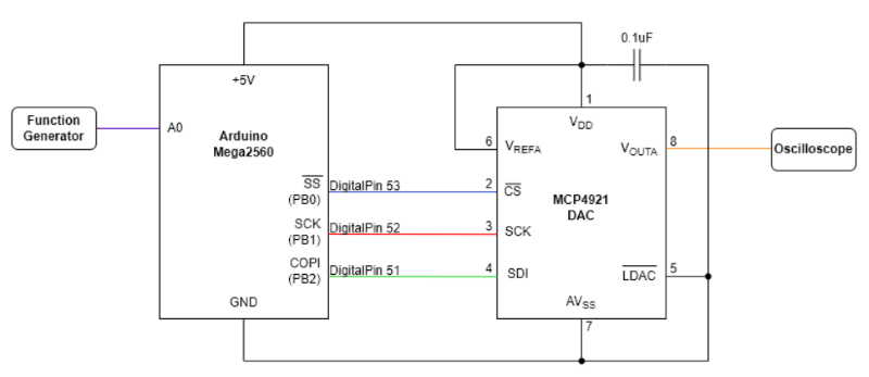
System Block Diagram with Circuit Connections
Physical Implementation
Program Code (Repository)
Results and Discussion
Conclusion
Theory
Analog-to-Digital Conversion (ADC)
Analog-to-digital conversion, also known as sampling, is the process of converting a continuous analog signal into a discrete digital signal. In general, an ADC system takes in, or “samples” the analog input at an interval determined by the sampling frequency, and converts the actual value to the closest discrete value.
Like the ATmega328P, the ATmega2560 features a 10-bit successive approximation ADC with +/- 2LSB absolute accuracy. A successive approximation ADC essentially compares the analog input voltage to the reference voltage by performing a binary search through all possible quantization levels until it converges on a digital output. Starting with the MSB, the ADC uses a sample and hold comparator to compare the analog input voltage \(V_{IN}\) with an internally generated reference voltage \(V_{ref,n}\ =\ (1/2)V_{REF}\). If the analog input voltage \(V_{IN}\) is greater than the internally generated reference voltage \(V_{ref,n}\), then the MSB is set to 1. Otherwise, it is set to 0. The process is repeated with the next lower bit, with the new internally generated reference voltage \(V_{ref,n+1}\ =\ (1/2)(V_{ref,n})\ +\ V_{ref,n}\) or \((1/2)(V_{ref,n})\) depending on the previous result, until the results converge, and the conversion is completed.
The minimum value of the ADC register (0x000) represents GND, and the maximum value (0x3FF) represents the reference voltage minus 1 LSB. For this experiment, the reference voltage is kept as the default \(A_{REF}\ =\ A_{VCC}\ =\ 5V\).
The resulting value is a normalized voltage found by:
\[ADC\ =\ \frac{V_{IN}(1024)}{V_{REF}}\]For \(V_{REF}\ =\ 5V\), this gives a resolution of 4.88mV per voltage step, or LSB. Since the maximum ADC value is the reference voltage minus 1 LSB, the maximum ADC value can be found to be:
\[(1024 - 1)(\frac{5}{1024})\ =\ 4.9951V\]Clock Rate
The ADC operates at a clock rate that is 16MHz / a ‘prescale factor’. By default, the prescale factor is set to 128, such that the clock rate = 16MHz / 128 = 125kHz. According to the data sheet, a normal conversion takes 13 ADC clock cycles. Therefore, the theoretical default sampling rate = 125kHZ / 13 ≈ 9600Hz. By changing the ADPS2, 1, 0 registers, the prescale factor can be changed, allowing the ADC to operate faster or slower. By writing ‘1 0 0’ to the ADPS2, 1, 0 registers respectively in the setup() function, the prescale factor can be changed to 16. While lower prescale factors are theoretically possible, the prescale factor is left at 16, as it is the lowest value that the ADC clock is rated for. The clock rate than becomes 16MHz / 16 = 1MHz. Using 13 ADC clock cycles per conversion, the sampling rate is theoretically found to be 1MHz / 13 ≈ 76.8kHz
Digital-to-Analog Conversion (DAC)
Digital-to-analog conversion is the process of converting a discrete digital signal into a continuous analog signal. In general, DAC uses interpolation to fill in the values between the steps of a digital signal in order to create a smoother analog signal. As the ATmega microcontrollers lack an onboard DAC accessible by the user, DAC must be performed by an external device. In this experiment, the MCP4921 IC is used. The MCP4921 is a 12-bit, single-channel DAC with SPI interface with up to 20MHz Clock Support.
1 LSB is the ideal voltage difference between two successive codes. The LSB size can be found by the following equation:
\[V_{OUT}\ =\ \frac{V_{REF}GD_N}{2^n},\]where G is the selected gain (1x in this case), DN is the digital input value, and n is the number of bits of resolution (n = 12).
System Block Diagram with Circuit Connections
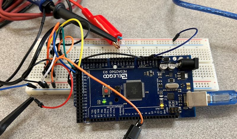
Physical Implementation
For the physical implementation of the system, power is supplied to the Arduino via the USB port. The MCP4921 is then powered by the 5V output pin from the Arduino. Because the Arduino cannot take negative voltage as input (max: -0.5V), the analog input signal from the function generator is given a DC offset of +2V, with Vp-p = 1V.
Program Code
The Arduino program code used is provided in the lab instructions with some minor adjustments. Since the Arduino Mega2560 is used, rather than the Arduino UNO, the pin declarations are changed to match the pinout of the Arduino Mega2560.
Additional code is also added to the original code to write to the ADC clock registers in order to increase the clock rate.
The full code is available in the repository here.
Results and Discussion
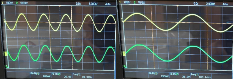
The ADC/DAC system is tested at various frequencies between 10 – 10kHz in order to observe the differences in the output due to clock rate/sampling frequency. For all results, the default clock rate input/output is shown in the left, and the faster clock rate input/output is shown on the right. It should be noted that due to technical issues with the oscilloscope probes, the amplitude shown are not accurate. However, they were tested to be experimentally equivalent.
At 10Hz and 100Hz, there is no noticable difference between the results obtained with the default clock rate and the faster clock rate. Both results show a faithful replication of the original input signal. However, at 1k+Hz, the difference in resolution due to the clock rate starts to become visible.
10Hz

100Hz
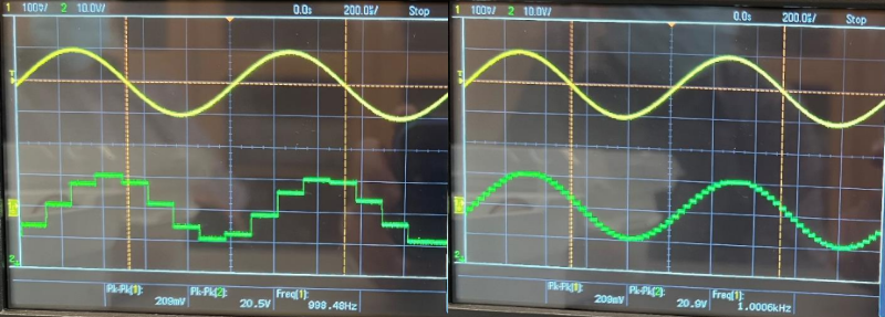
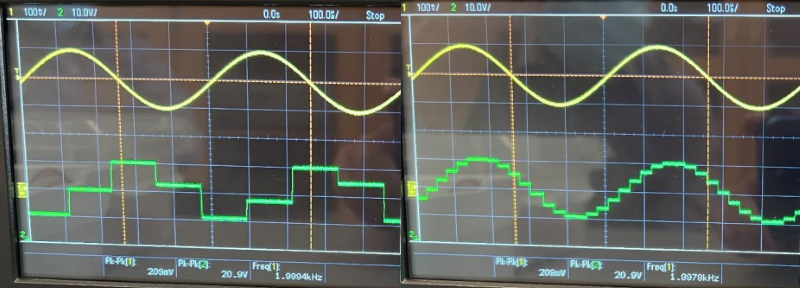
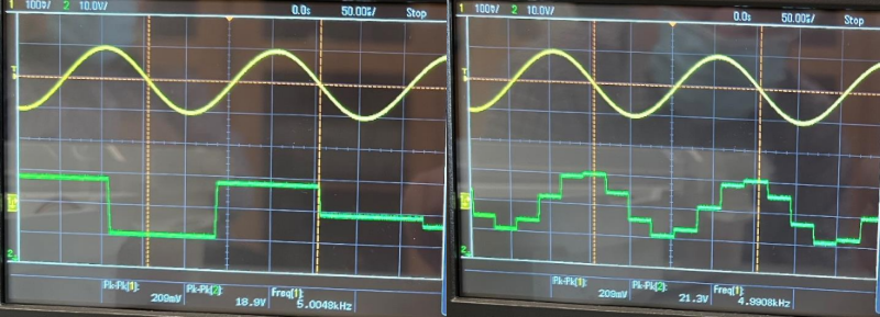
Starting at 1kHz, the default clock rate-sampled output starts to become unable to replicate the sine wave. Freezing the frame of the oscilloscope allows for the observation of the characteristic staircase shape of a digital signal. The faster clock rate-sampled output is able to maintain roughly the shape of a sine wave for up to about 5kHz, by which point the default clock rate-sampled output can be seen to have already lost its symmetry and structure.
1kHz
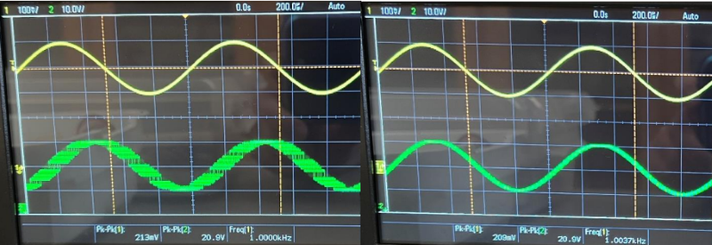
1kHz (paused)
2kHz (paused)
5kHz (paused)
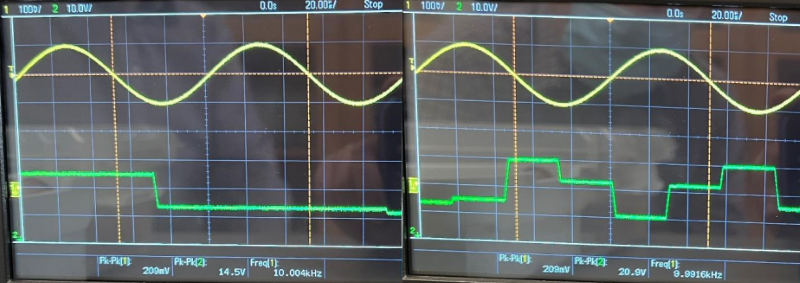
Increasing the input frequency up to 10kHz, even the faster clock rate is no longer able to maintain the symmetry. The default clock rate, of course, looks even less like the original intput signal.
10kHz

10kHz (paused)
Conclusion
In this lab experiment, an ADC-DAC system was implemented on an Arduino Mega 2560 in conjunction with an MCP4921 IC chip to convert an analog input signal into digital values and then back into an analog output signal. The effect of the clock rate on the sampling process was also seen by comparing the results using the default clock rate and a faster clock rate.
From the results, it can be seen that the system was properly implemented. By supplying an analog sine wave as the input signal, the system was able to convert the analog signal into digital values, and then convert the digital values back into an analog signal to be outputted to the oscilloscope. It can be seen that the system was better able to replicate the input signal at lower frequencies. However, when the signal frequency is increased, the resulting signal became less and less accurate.
By changing the prescale factor, the clock rate of the ADC clock can be changed to increase or decrease the sampling frequency. The effects of this change in sampling frequency can also be seen in the results, especially at higher frequencies, where the outputs start to look less and less like sine waves. Depending on the application, which would determine the acceptability of the results, the maximum input frequency at which the default clock rate is able to replicate the input sine wave is ≤ 1kHz, likely at a frequency closer to 100Hz. For the faster clock rate, the highest frequency appears to be around 2k - 5kHz.