Analog Lead Compensator Circuit
Project Overview
Part 1 of Benchtop Labs for Digital Control course.
The purpose of this lab experiment is to model a satellite in the analog domain as a double integrator using op amps. As a double integrator is inherently unstable, an analog controller must be added to the system. In this experiment, a lead compensator is to be used as the controller for this system.
Index
Op-Amp Selection
Plant
Compensator
Summing Junction
Variable Gain Stage
Level Shifter
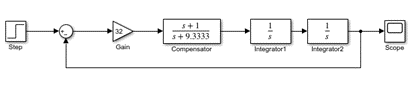
Simulation (Simulink)
Results and Discussion
Conclusion
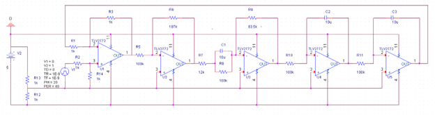
Appendix A: Full Schematic Diagram
Op-Amp Selection
For this experiment, the TLV2774 op-amp, manufactured by Texas Instruments, was chosen to implement this circuit. This component was one of the op-amps suggested by the lab instructions for use in this experiment. The TLV2774 is a single-supply, rail-to-rail op-amp, with supply voltage from 0 – 6V.
Plant
Design
In the frequency domain, an integrator has the transfer function 1/s. A double integrator therefore has the transfer function 1/s^2. The transfer function of an inverting op amp integrator is given by \(G\left(s\right)=\frac{1}{sRC}\). For unity gain, RC = 1. To avoid overly large values for R or C, C was chosen to be 10µF, making R = 100kΩ.
Circuit

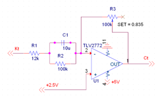
Compensator
Design
From the lab instruction, the transfer function of the lead compensator is given as
\[C(s)\ =\ k\frac{\left(s+1\right)}{\left(s+10\right)}\]The circuit design of a lead compensator was found in Design of Feedback Control Systems, 4th ed., by Stefani, Shahian, Savant, and Hostetter, with the following parameters.

Comparing with our desired transfer function, b = 1, and a = 10. Again, component values were chosen as C1 = 10µF, and R2 = 100kΩ, such that
\[b\ =\ \frac{1}{\left(100\times{10}^3\right)\left(10\times{10}^{-6}\right)}\ =\ 1\]Solving for R1,
\[10\ =\ \left(1+\frac{\left(100\times{10}^3\right)}{R_1}\right)\left(1\right)\] \[9\ =\ \frac{\left(100\times{10}^3\right)}{R_1}\] \[R_1\ =\ \frac{\left(100\times{10}^3\right)}{9}\ \cong\ 11.111k\Omega\]Originally, a 10kΩ resistor and a 1kΩ resistor were placed in series to create an equivalent resistance of 11kΩ. However, the experimental result had a small steady state error which was not correctable by varying the gain. Replacing the equivalent resistors with a single 12kΩ resistor eliminated the steady state error. The tradeoff was that the pole of the compensator was also affected, moving from -10 to -9.333.
Instead of a fixed-value feedback resistor, a 100kΩ potentiometer was used to allow for variable gain adjustment. The value for the potentiometer was experimentally determined by examining the response of the system, and found to be 83.5kΩ.
Circuit
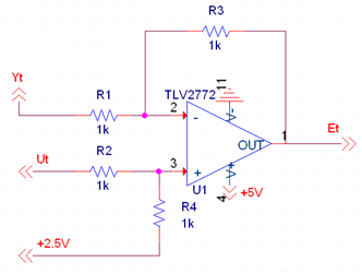
Summing Junction
Design
The summing junction is a differential amplifier implemented with an op-amp. The output of a differential amplifier is given by
\[V_{out}\ =\ V_+\left(\frac{R_4}{R_2+R_4}\right)\left(\frac{R_1+R_3}{R_1}\right)-V_-\left(\frac{R_3}{R_1}\right)\]For \(R_1=R_2=R_3=R_4=1k\Omega\):
\[V_{out}\ =\ V_+-V_-\ =\ U\left(t\right)-Y\left(t\right)=E\left(t\right)\]The summing junction/differential amplifier produces an output that is the difference between the two inputs. When the inputs are the set point and the feedback signal from the output of the circuit, the summing junction produces the error signal, which is fed into the compensator.
Circuit
Variable Gain Stage
Design
To allow for further adjustment of the gain, a variable gain stage is added between the summing junction and the compensator. It is implemented by a simple inverting amplifier with a potentiometer as the feedback resistor. The output is given by \(V_{out}\ =\ -V_{in}\left(\frac{R_2}{R_1}\right)\)
The value of the potentiometer was again experimentally determined by examining the response of the system, and found to be 187kΩ.
Circuit

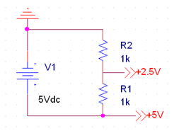
Level Shifter
Design
Because the single-supply op amp has only positive voltage, while the input signal has both positive and negative voltage, a reference voltage of +2.5V was created by implementing a voltage divider across the DC power supply, to allow the signal to have both a positive and negative swing. This shifts the DC level of the circuit up by +2.5V, such that the range of the circuit becomes -2.5V - +2.5V.
Circuit
Simulation (Simulink)
Model
Simulation Plot
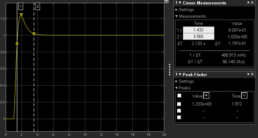
Rise time: 1.432 - 1.079 = 0.353s
Settling time: 3.565s
Percent overshoot: 23.3%
Results and Discussion
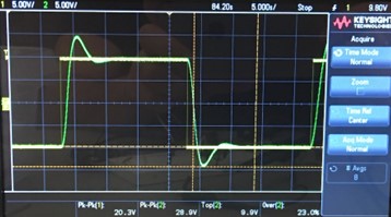
Rise time: ~2s
Settling time: ~7.5s
Percent overshoot: 23%
It should be noted that due to technical issues with the oscilloscope probes, the amplitude shown are ~10x the actual value.
Comparing the results from the simulation and the analog circuit, it can be seen that the rise time and settling time were much higher with the circuit. However, the percent overshoot was actually almost the same. Additionally, while in simulation, a gain of 32 was found to give the best response (smallest overshoot and fast settling time), this did not turn out to be the case with the analog circuit. Reducing the overshoot was prioritized when adjusting the gain in the circuit using the two potentiometers. The overall gain of the system that produced the least overshoot was found to be about 13.
The main deficiency of this circuit design was the speed of the response. Attempts were made to improve the speed by varying the gain, but to no avail. Because the response of the circuit was so slow, it was necessary for the input from the waveform generator to be at a very low frequency, < 0.0625Hz. At higher frequencies, the output would not have enough time to settle. This also made tuning the gain of the system much more difficult, as it would take a long time to see how any adjustments affected the response. One possible reason could be due to the fact that single-supply op-amps were used in this design.
Conclusion
This analog circuit design fulfilled its overall purpose of implementing a double integrator plant, as well as a lead compensator to control the unstable double integrator signal. However, the slow speed of its response was a major deficiency, limiting the frequencies at which the circuit can serve its function. In future design iterations, changing from the use of single-supply op amps to dual-supply op amps could be a significant step towards improving the performance of the circuit.
Appendix A
Full Schematic Diagram